Processing
Element
Processing
Element
The Multiplus Processing Element is based on the use of SPARC processors. The first
implementation of the processing element used the Cypress SPARC chipset and could support
a 64-Kbyte cache and up to 32 Mbytes of memory belonging to the global address
space. The
most recent implementation of the Processing Element can have up to 2 SuperSPARC II
modules running at 85 Mhz and supporting a 1 MB Cache. This new Processing Element can
support up to 256 Mbytes of memory. In addition to the SPARC processors and
memory, the Multiplus Processing Element includes: ROM, serial interface, interrupt registers and
timers.
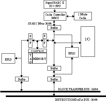
The previous figure shows a block diagram of the current Processing
Element architecture which is built around any SPARC MBUS module. Only a single SPARC
module is represented in Figure 2. The number of address lines followed by the number of
data lines is annotated next to every bus. The cache controller works in write-through
mode with invalidation of shared cache copies, which is a very simple approach and has
proved to be as efficient as the write-back mode in simulation experiments carried out
considering typical values for the data cache hit rate and the rate of write
operations.
The control logic of the Processing Element is implemented with the use of
four EPLDs. The first one performs the slave function in the Block Transfer Bus,
arbitrates the use of the common bus for memory access within the processing element and
performs the DRAM control. The address decodification in the Block Transfer Bus is
performed by another EPLD. In the control of the instruction/data section, two EPLDs are
used. The first one performs address decoding and access control to the processing element
registers and I/O devices. The second one performs the master and slave functions in the
Instruction/Data Bus and the arbitration between requests issued by the
Instruction/Data
Bus and by the Processing Element Data Cache Controller.
Within the memory, a TAG bit is associated with each memory data block in
order to indicate if a copy of this block may exist in another cache. The bit is set
whenever the block is read by a different processing element sitting within the same
cluster. It is reset whenever that block is rewritten by the local processing
element. The
importance of this bit is to reduce the need for broadcasting unnecessary data access to
the Instruction/Data Bus in order to maintain cache consistency. If the TAG bit is not
set, the data access can be performed within the Processing Element and without the use of
the Instruction/Data Bus.