Multiplus
Architecture
Multiplus
Architecture
Multiplus is a distributed shared-memory high-performance computer designed to have a
modular architecture which is able to support up to 1024 processing elements and 32 Gbytes
of global memory address space. Figure shows the Multiplus basic architecture. Within
Multiplus, up to eight processing elements can be interconnected through a 64-bit
double-bus system making up a cluster. Each bus follows a similar protocol to the one
defined for the SPARC MBUS, but is implemented as an asynchronous bus.
The Multiplus architecture supports up to 128 clusters interconnected through an
inverted n-cube multistage network. Through the addition of processing elements and
clusters, the architecture can cover a broad spectrum of computing power, ranging from
workstations to powerful parallel computers. With the adopted structure, the cost and
delay introduced by the interconnection network is small or even non-existent in the
implementation of parallel computers with up to 64 processing elements. On the other
hand,
very large parallel computers can be built without the use of an extremely expensive or
slow interconnection network.
The Multiplus architecture can be classified as a Non-Uniform Memory Access (NUMA)
architecture since a processing element access to memory can be performed in four
different ways. The fastest memory access is a direct read operation on the local
caches,
which is performed within a processor cycle. The second fastest memory access is any
read/write operation within the local bank of memory since, in principle, it does not
require the use of the cluster bus system for its completion. The third fastest memory
access is a write or a read access with cache failure to a memory position belonging to an
external memory bank within the same cluster. In this case, the bus system must be used
and the bus arbitration time is added to the access time.
Lastly, there are the accesses generated by a processing element requesting information
which is not in its local caches but is stored within a memory bank sitting on another
cluster. In this case, the bus system of the source cluster, the multistage
interconnection network and the bus system of the destination cluster need to be used for
the access operation to be performed. Therefore, the arbitration times of both bus systems
and the multistage interconnection network delay are added to the access time.
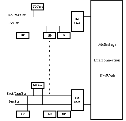
As shown in the above figure, Multiplus uses a distributed I/O system
architecture. It is possible to assign all processing elements within a cluster to a
single I/O processor which is responsible for dealing with all I/O requests to or from
mass storage devices started by these processing elements.
Design decisions have been taken to simplify the problem of maintaining consistency
among the private caches of the processing elements within the Multiplus
architecture. The
first one is to have in every cluster one bus dedicated to instruction and data access
operations and the other one dedicated to block transfer operations which occur in I/O or
in memory page migration or copy operations. Only the instruction/data bus needs to be
"snooped" by the cache controller and, as a result, the cache consistency
problem can be solved within a cluster with the methods usually adopted in bus-based
systems. In addition, a software approach has been adopted to keep cache consistency
between clusters. Following the memory model based on the lazy release consistency
approach, any access to shared regions of memory must be preceded by a "lock"
operation. This ensures that a single processor is accessing a particular critical region
at any moment. Cache consistency is achieved with the help of the memory management
hardware.