I/O
Processor
I/O
Processor
The architecture of the Multiplus I/O Processor is shown in the following figure. It
consists of two bus systems: the CPU Bus and the DMA Bus. Attached to each bus there is a
68020 CPU. The one associated with the CPU Bus is responsible for managing the I/O
requests sent by the processing elements to the 16 Kbytes dual-port Command Memory, for
performing the Disk Cache control, for sending commands to be executed by the devices on
the DMA Bus through the 4 Kbytes Communication Memory and for controlling a serial
interface. It uses a 4 Mbytes RAM for its work area and a 64 Kbytes ROM to store the
initialization procedure.
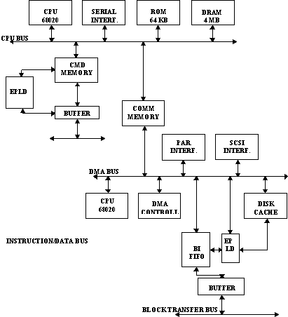
The CPU on the DMA Bus controls the execution of the internal tasks issued
by the CPU Bus through the Communication Memory. Attached to the DMA Bus there are: a SCSI
interface for the connection of disks, tapes and floppies; a Parallel Interface for the
connection of printers; a 32 Mbytes write-through Disk Cache; a DMA Controller which is
responsible for the data transfer from the SCSI and Parallel Interface to the Disk Cache;
and an 8 Kbytes BIFIFO which is used as a temporary storage to transmit data between the
Disk Cache and the processing elements through the Block Transfer Bus.
Two EPLDs are used to perform some control functions within the I/O Processor. The
first one performs the master/slave functions on the Instruction/Data Bus. The second one
performs the master/slave functions on the Block Transfer Bus and controls the burst data
transfers between the Disk Cache and the BIFIFO on the DMA Bus.

The operation of the I/O Processor is started when a Processing Element
writes an I/O command into its assigned region within the Command Memory. This generates
an interrupt to the CPU Bus 68020 which, then, interprets the command and, if necessary,
splits it into sub-tasks that will be performed by the I/O Processor hardware attached to
the DMA Bus. For instance, if the command is a disk block read operation, the CPU Bus
68020 firstly checks if the block is stored within the Disk Cache. If it is, a command to
transfer the block from the cache to the processing element memory is issued to the DMA
Bus through the Communication Memory. Otherwise, the command is split into two tasks: the
reading of data from the disk to the cache under the supervision of the DMA Controller and
the data transfer from the cache to the Processing Element memory through the BIFIFO under
the control of the EPLD. Again, both tasks are issued to the DMA Bus through the
Communication Memory. Once all steps of a Processing Element command have been executed by
the DMA Bus, the CPU Bus does a write operation to the interrupt register of the
Processing Element through the Instruction/Data Bus.